PCB Design vs VLSI Design: Key Differences, Applications, and Career Scope
PCB Design vs VLSI Design – In the world of electronics and semiconductor engineering, PCB Design vs VLSI Design are two essential fields that play a major role in building modern electronic devices. From smartphones and laptops to medical equipment and satellites, these technologies work together to make complex electronic systems possible.
Although both involve circuit design and electronic components, PCB design vs VLSI design serve very different purposes in the electronics development process. PCB design focuses on connecting components on a physical board, while VLSI design focuses on creating integrated circuits (ICs) with millions or even billions of transistors on a single chip.
In this article, we will explore PCB design vs VLSI design, how they work, their tools, applications, and career opportunities.
What is PCB Design?
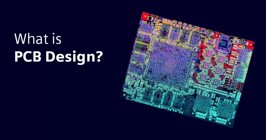
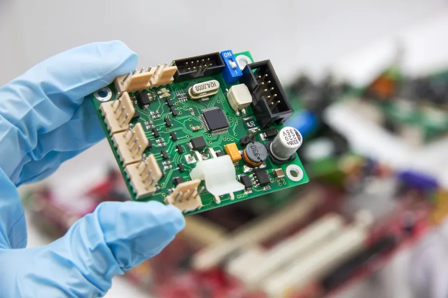
Printed Circuit Board (PCB) design is the process of designing the physical layout of electronic circuits on a board that connects electronic components such as resistors, capacitors, microcontrollers, and integrated circuits.
A PCB acts as the foundation that holds and electrically connects all components in an electronic system. Designers create conductive pathways (called traces) on copper layers to ensure signals and power flow correctly between components.
Key Elements of PCB Design
- Schematic Design – Creating the electrical circuit diagram.
- Component Placement – Arranging components on the board.
- Routing – Designing copper traces that connect components.
- Layer Stackup – Determining the number of PCB layers.
- Design Rule Check (DRC) – Ensuring the design meets manufacturing standards.
Common PCB Design Tools
Some widely used PCB design tools include:
- Altium Designer
- KiCad
- Autodesk Eagle
- OrCAD
Applications of PCB Design
PCB boards are used in nearly every electronic device, such as:
- Consumer electronics (smartphones, TVs, laptops)
- Automotive electronics
- Medical devices
- Industrial automation systems
- Communication equipment
What is VLSI Design?
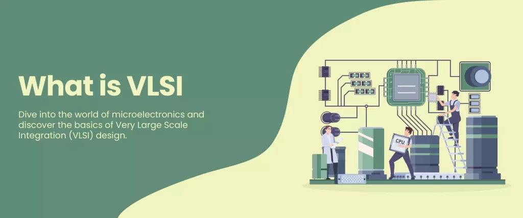
Very Large Scale Integration (VLSI) design is the process of designing integrated circuits (ICs) by combining millions or billions of transistors onto a single semiconductor chip.
VLSI technology is responsible for creating powerful chips used in processors, memory devices, and system-on-chip (SoC) architectures.
Instead of designing a physical board like PCB design, VLSI engineers design circuits at the semiconductor level, working with logic gates, transistors, and digital circuits.
Major Stages of VLSI Design
- Specification – Defining the functionality of the chip.
- RTL Design – Designing digital circuits using hardware description languages.
- Simulation & Verification – Testing the design behavior.
- Synthesis – Converting RTL into gate-level representation.
- Physical Design – Creating layout of transistors and interconnections.
- Fabrication – Manufacturing the chip using semiconductor processes.
Common VLSI Design Tools
Some popular tools used in VLSI design include:
- Cadence Virtuoso
- Synopsys Design Compiler
- Mentor Graphics
- Xilinx Vivado
Applications of VLSI Design
VLSI chips power modern technology including:
- Microprocessors
- Graphics processing units (GPUs)
- Memory chips (RAM, ROM)
- Artificial intelligence accelerators
- Embedded systems
PCB Design vs VLSI Design: Key Differences
| Feature | PCB Design | VLSI Design |
|---|---|---|
| Definition | Designing circuit boards that connect electronic components | Designing integrated circuits with millions of transistors |
| Design Level | System / board level | Chip / semiconductor level |
| Components | Uses ICs, resistors, capacitors, connectors | Uses transistors, logic gates |
| Complexity | Moderate complexity | Extremely high complexity |
| Manufacturing | PCB fabrication and assembly | Semiconductor wafer fabrication |
| Design Tools | Altium, KiCad, Eagle | Cadence, Synopsys |
| Application | Hardware devices and circuit boards | Processors and microchips |
Workflow Comparison
PCB Design Workflow
- Circuit schematic creation
- Component selection
- PCB layout design
- Routing and signal optimization
- Design rule verification
- Manufacturing and assembly
VLSI Design Workflow
- Chip architecture design
- RTL coding (using HDL)
- Functional verification
- Logic synthesis
- Physical design and layout
- Chip fabrication
Skills Required for PCB Design
PCB designers typically require knowledge in:
- Electronic circuit fundamentals
- Analog and digital electronics
- Signal integrity
- PCB layout rules
- Hardware debugging
Additional skills include working with CAD tools and understanding component datasheets.
Skills Required for VLSI Design

VLSI design requires deeper knowledge of semiconductor and digital design concepts, including:
- Digital logic design
- Semiconductor physics
- Hardware description languages (HDL)
- Timing analysis
- Chip architecture
- Verification techniques
Programming skills in languages such as Verilog or VHDL are often required.
Career Opportunities
Both fields offer strong career opportunities in the electronics and semiconductor industries.
PCB Design Careers
Common job roles include:
- PCB Design Engineer
- Hardware Design Engineer
- Embedded Hardware Engineer
- Electronics Design Engineer
Industries hiring PCB designers include consumer electronics, automotive, aerospace, and robotics.
VLSI Design Careers
VLSI professionals often work in semiconductor companies with roles such as:
- VLSI Design Engineer
- ASIC Design Engineer
- FPGA Engineer
- Verification Engineer
Major semiconductor companies like Intel, Qualcomm, NVIDIA, and Texas Instruments hire VLSI engineers.
Which One Should You Choose?

Choosing between PCB design and VLSI design depends on your interests and career goals.
- If you enjoy working with electronic hardware, circuits, and board-level systems, PCB design might be a better fit.
- If you are interested in chip architecture, digital logic, and semiconductor technology, VLSI design could be the ideal path.
PCB design typically focuses on practical hardware implementation, while VLSI design focuses on advanced semiconductor technology and chip design.
Conclusion
PCB design and VLSI design are both essential components of modern electronics engineering. While PCB design deals with building and connecting electronic components on circuit boards, VLSI design focuses on creating complex integrated circuits at the semiconductor level.
Together, these technologies power everything from everyday consumer gadgets to advanced computing systems. Understanding the differences between PCB and VLSI design helps engineers choose the right specialization and contributes to building innovative electronic products.
As technology continues to evolve, the demand for skilled engineers in both PCB design and VLSI design will continue to grow, making them valuable and rewarding career paths in the electronics industry.
Want to Learn More??, Kaashiv Infotech Offers, VLSI Internship, IOT Internship & More, Visit Their website course.kaashivinfotech.com.